Dataset for Structural and optical emission uniformity of m-plane InGaN single quantum wells in core-shell nanorods
Controlling the long-range homogeneity of core-shell InGaN/GaN layers is essential for their use in light-emitting devices. Understanding the impact of the crystallographic arrangement and material composition on light emission at a nanometer scale is a key feature for the fabrication of efficient light emitting devices. We investigated the structural quality and composition of the material via Transmission Electron microscopy (TEM) and Energy Dispersive X-ray (EDX) spectroscopy. The light emission were qualitatively assessed via Hyperspectral Cathodolumiscence (CL) spectroscopy. We use these information to determine the impact of the composition inhomogeneities on light emission. We have found that a homegeneous long-range light emission can be achieved on InGaN/GaN core-shell structure despite the presence of nano-scale alloy compositional fluctuations.
This dataset contains the results of scanning electron microscopy (SEM), transmission electron microscopy (TEM) and Energy Dispersive X-ray (EDX) measurements carried out on InGaN/GaN core-shell nanostructures. The samples are highly regular arrays of GaN plasma etched cores onto which wide InGaN layer capped with a GaN layer were grown using different metal organic vapour phase epitaxy (MOVPE) growth parameters.
Three different growth temperature were used to grow the InGaN layer: 750°C, 700°C and 650°C. SEM images were used to characterize the describe the fabrication, growth and assess nanorod morphologies. TEM were used to investigate the structural properties and assess the InGaN thickness along the entire length of the m-plane facets. EDX measurements were used to assess the homogeneity of the InGaN layer composition at different position along the m-plane facet and on the semi-polar facets.
Cite this dataset as:
Le Boulbar, E.,
Hosseini Vajargah, S.,
Edwards, P.,
Griffiths, I.,
Girgel, I.,
Coulon, P.,
Cherns, D.,
Martin, R.,
Humphreys, C.,
Bowen, C.,
Allsopp, D.,
Shields, P.,
2016.
Dataset for Structural and optical emission uniformity of m-plane InGaN single quantum wells in core-shell nanorods.
Bath: University of Bath Research Data Archive.
Available from: https://doi.org/10.15125/BATH-00150.
Export
Data
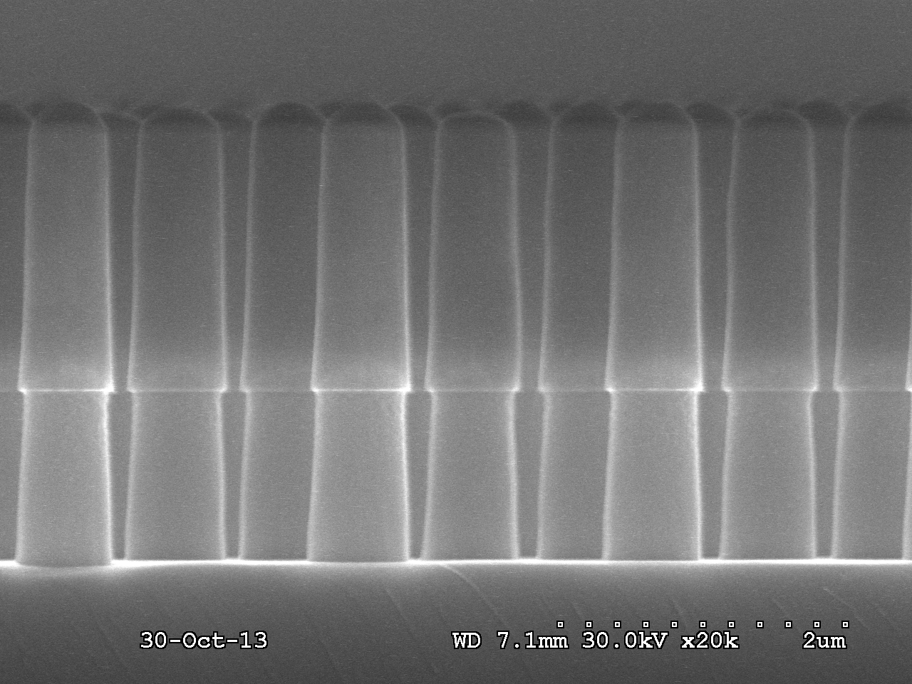
GaN_Nanorod … cross_section.bmp
image/x-ms-bmp (1MB)
Creative Commons: Attribution 4.0
SE image used in Fig1
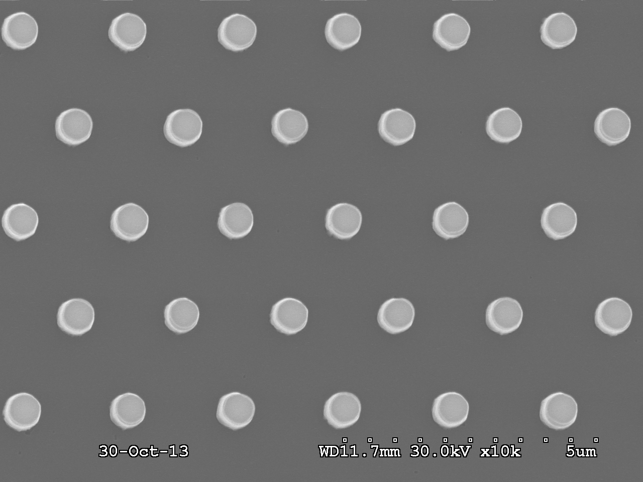
GAN_Nanorod_template_planar.bmp
image/x-ms-bmp (1MB)
Creative Commons: Attribution 4.0
SE image used in Fig1
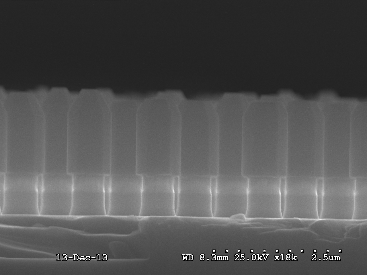
Faceted_GaN … cross_section.bmp
image/x-ms-bmp (1MB)
Creative Commons: Attribution 4.0
SE images used in Fig. 2
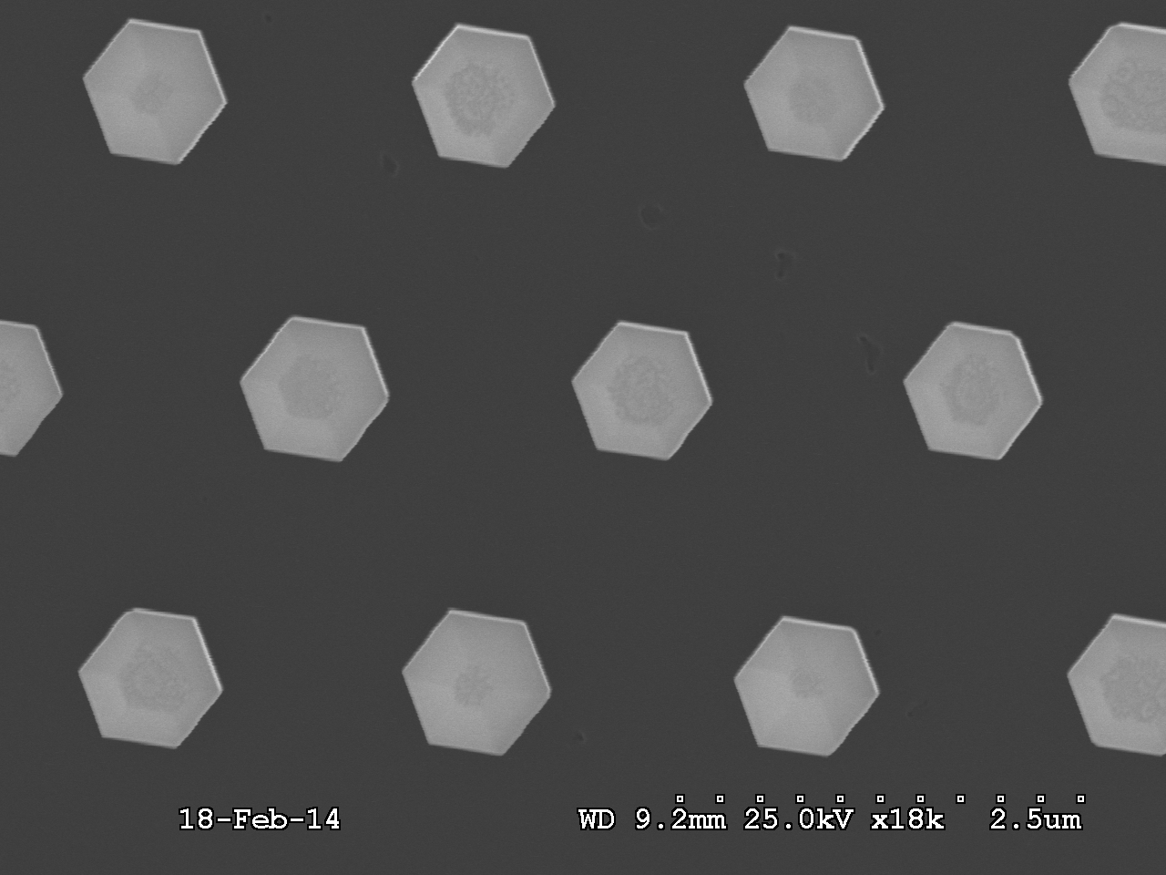
Faceted_GaN_Nanorod_planar.bmp
image/x-ms-bmp (1MB)
Creative Commons: Attribution 4.0
SE images used in Fig. 2
TEM_image_HAADF … semipolar.bmp
image/bmp (1MB)
Creative Commons: Attribution 4.0
HAADF STEM image of the radial InGaN/GaN core-shell structure grown at 650°C used in Figure 3. a)
TEM_image_HAADF … and_top.bmp
image/bmp (1MB)
Creative Commons: Attribution 4.0
HAADF STEM image of the radial InGaN/GaN core-shell structure grown at 650°C used in Figure 3. a) and b)
TEM_image_HAADF__top.bmp
image/bmp (1MB)
Creative Commons: Attribution 4.0
HAADF STEM image of the radial InGaN/GaN core-shell structure grown at 650°C used in Figure 3. a)
TEM_image_HAADF__middle.bmp
image/bmp (1MB)
Creative Commons: Attribution 4.0
HAADF STEM image of the radial InGaN/GaN core-shell structure grown at 650°C used in Figure 3. a) and c)
TEM_image_HAADF__base.bmp
image/bmp (1MB)
Creative Commons: Attribution 4.0
HAADF STEM image of the radial InGaN/GaN core-shell structure grown at 650°C used in Figure 3. a) and d)
fig4a_InN_content … 650degC.xlsx
application/vnd.openxmlformats-officedocument.spreadsheetml.sheet (16kB)
Creative Commons: Attribution 4.0
Figure 4 a): Raw data used to plot the indium map of the wide InGaN SQW obtained by EDX on {1-101} plane at 650°C growth
fig4b_InN_content … 700degC.xlsx
application/vnd.openxmlformats-officedocument.spreadsheetml.sheet (18kB)
Creative Commons: Attribution 4.0
Figure 4 b): Raw data used to plot the indium map of the wide InGaN SQW obtained by EDX m-plane at 700°C growth
fig4c_InN_content … 650degC.xlsx
application/vnd.openxmlformats-officedocument.spreadsheetml.sheet (20kB)
Creative Commons: Attribution 4.0
Figure 4 c): Raw data used to plot the indium map of the wide InGaN SQW obtained by EDX m-plane at 650°C growth
fig5b_Mean … 650degC_semipolar.xlsx
application/vnd.openxmlformats-officedocument.spreadsheetml.sheet (11kB)
Creative Commons: Attribution 4.0
Figure 5 b): Raw data used to plot the average InN contents measured using EDX at different positions along the {1-101} grown at 650°C
fig5c_Mean … error_700degC.xlsx
application/vnd.openxmlformats-officedocument.spreadsheetml.sheet (11kB)
Creative Commons: Attribution 4.0
Figure 5 c): Raw data used to plot the average InN contents measured using EDX at different positions along the m-plane facets grown at 700°C
fig5d_Mean … error_650degC.xlsx
application/vnd.openxmlformats-officedocument.spreadsheetml.sheet (12kB)
Creative Commons: Attribution 4.0
Figure 5 c): Raw data used to plot the average InN contents measured using EDX at different positions along the m-plane facets grown at 650°C
Fig6a_SEM_image_750degC.tif
image/tiff (976kB)
Creative Commons: Attribution 4.0
SE image of the InGaN/GaN core-shell grown at 750°C used in figure 6 a)
Fig6b_SEM_image_700degC.tif
image/tiff (976kB)
Creative Commons: Attribution 4.0
SE image of the InGaN/GaN core-shell grown at 700°C used in figure 6 b)
Fig6c_SEM_image_650degC.tif
image/tiff (976kB)
Creative Commons: Attribution 4.0
SE image of the InGaN/GaN core-shell grown at 650°C used in figure 6 c)
fig6d_rawdata.txt
text/plain (200kB)
Creative Commons: Attribution 4.0
Figure 6 d): Raw data extracted from the hyperspectral dataset used to plot the CL intensity image
fig6e_rawdata.txt
text/plain (200kB)
Creative Commons: Attribution 4.0
Figure 6 e): Raw data extracted from the hyperspectral dataset used to plot the CL intensity image
fig6f_rawdata.txt
text/plain (351kB)
Creative Commons: Attribution 4.0
Figure 6 f): Raw data extracted from the hyperspectral dataset used to plot the CL intensity image
fig6g_rawdata.txt
text/plain (354kB)
Creative Commons: Attribution 4.0
Figure 6 g): Raw data extracted from the hyperspectral dataset used to plot the CL intensity image
fig6h_rawdata.txt
text/plain (352kB)
Creative Commons: Attribution 4.0
Figure 6 h): Raw data extracted from the hyperspectral dataset used to plot the CL intensity image
fig6i_rawdata.txt
text/plain (354kB)
Creative Commons: Attribution 4.0
Figure 6 h): Raw data extracted from the hyperspectral dataset used to plot the CL intensity image
Fig6j_meanspectrum_alltemp.xlsx
application/vnd.openxmlformats-officedocument.spreadsheetml.sheet (73kB)
Creative Commons: Attribution 4.0
Figure 6 j): Raw data related to the area-averaged, room-temperature CL spectra from the samples grown at 750°C, 700°C and 650°C
Fig6k_Rodtorodu … 700deg.xlsx
application/vnd.openxmlformats-officedocument.spreadsheetml.sheet (108kB)
Creative Commons: Attribution 4.0
Figure 6 k): Raw data related to the m-plane emission peak of multiple individual nanorods for samples grown 700°C
Fig6l_Rodtorodu … 650deg.xlsx
application/vnd.openxmlformats-officedocument.spreadsheetml.sheet (108kB)
Creative Commons: Attribution 4.0
Figure 6 l): Raw data related to the m-plane emission peak of multiple individual nanorods for samples grown 650°C
Fig7a_linescan … 31_43_132.txt
text/plain (704kB)
Creative Commons: Attribution 4.0
Figure 7 a): Raw data used to plot the CL spectra as a function of the position along the GaN/InGaN nanorod for the sample grown at 750°C
Fig7b_linescan … 11_55_39.txt
text/plain (208kB)
Creative Commons: Attribution 4.0
Figure 7 b): Raw data used to plot the CL spectra as a function of the position along the GaN/InGaN nanorod for the sample grown at 700°C
Fig7c_linescan … 0_130_70.txt
text/plain (517kB)
Creative Commons: Attribution 4.0
Figure 7 b): Raw data used to plot the CL spectra as a function of the position along the GaN/InGaN nanorod for the sample grown at 650°C
Fig7d_resonance_raw_data.xlsx
application/vnd.openxmlformats-officedocument.spreadsheetml.sheet (60kB)
Creative Commons: Attribution 4.0
Raw data related to individual spectra from different positions along the m-plane of a single nanorod from the 650°C sample used in figure 7 d)
fig8a_750deg_rawdata.xlsx
application/vnd.openxmlformats-officedocument.spreadsheetml.sheet (12kB)
Creative Commons: Attribution 4.0
Figure 8 a): Raw data centroid emission energy measured along the length of several nanorod m-plane facets for growth at 750°C taken at room temperature
fig8b_700deg_rawdata.xlsx
application/vnd.openxmlformats-officedocument.spreadsheetml.sheet (13kB)
Creative Commons: Attribution 4.0
Figure 8 b): Raw data centroid emission energy measured along the length of several nanorod m-plane facets for growth at 700°C taken at room temperature
fig8c_650deg_rawdata.xlsx
application/vnd.openxmlformats-officedocument.spreadsheetml.sheet (13kB)
Creative Commons: Attribution 4.0
Figure 8 a): Raw data centroid emission energy measured along the length of several nanorod m-plane facets for growth at 650°C taken at room temperature
Fig9_rawdata.xlsx
application/vnd.openxmlformats-officedocument.spreadsheetml.sheet (12kB)
Creative Commons: Attribution 4.0
InN fraction obtained from EDX map and Vegard's law raw data used to plot figure 9
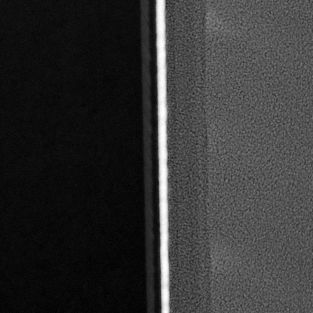
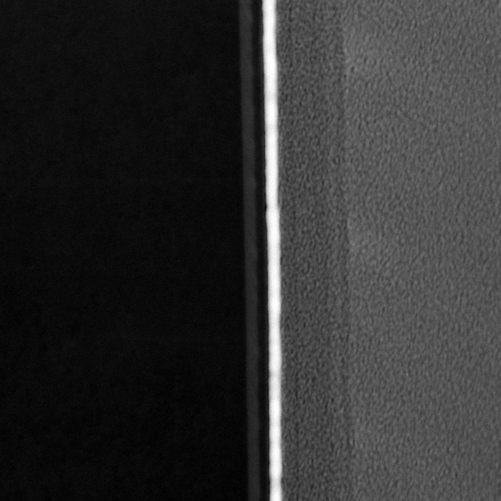
Fig3e_HRTEM_700degC.bin.tif
image/tiff (1MB)
Creative Commons: Attribution 4.0
Atomic resolution image of the m-plane InGaN/GaN interface for the sample grown at 700°C
Fig3e_inset … fourier_transform.tif
image/tiff (1MB)
Creative Commons: Attribution 4.0
Fourier transform of the atomic resolution image of the m-plane InGaN/GaN interface for the sample grown at 700°C. Image used for Fig. 3e inset.
Creators
Emmanuel Le Boulbar
University of Bath
Shahrzad Hosseini Vajargah
University of Cambridge
Paul Edwards
Researcher
University of Strathclyde
Ian Griffiths
University of Bristol
Ionut Girgel
University of Bath
Pierre-Marie Coulon
University of Bath
David Cherns
Researcher
University of Bristol
Robert W. Martin
Researcher
University of Strathclyde
Colin J. Humphreys
University of Cambridge
Chris Bowen
University of Bath
Duncan Allsopp
Researcher
University of Bath
Philip Shields
Researcher
University of Bath
Contributors
University of Bath
Rights Holder
Documentation
Data collection method:
Secondary electron images were captured using a Hitachi S-4300 scanning electron microscope (SEM). An accelerating voltage of 5 kV was used to collect the images. Atomic resolution STEM images were acquired using a FEI TITAN 80-300 microscope that was equipped with a CEOS CESCOR spherical aberration (Cs) corrector in the probe forming lens and high-brightness FEI XFEG electron source. Atomic resolution HAADF STEM images were acquired at an accelerating voltage of 300 keV and probe convergence semi-angle of 17.9 mrad and col-lection semi-angle of 55-200 mrad. Energy dispersive X-Ray spectroscopy analyses were carried out using FEI Tecnai Osiris. This microscope was equipped with XFEG and Super X system EDS detectors. This detector comprises 4 Bruker silicon detectors (SDD) arranged symmetrically around the optic axis of the microscope for high collection efficiency and high count rate. Spectrum images were acquired at a spatial sampling of 2 nm/pixel and 1 s/pixel dwell times with a probe current of approximately 0.5 nA, at an accelerating voltage of 200 keV.
Data processing and preparation activities:
Samples for TEM were prepared by a dual beam focused ion beam system. The nanorods were protected by a platinum layer prior to etching to reduce damage that could occur with the use of ion beam system. The samples for EDX measurements and atomic resolution STEM were prepared by a tripod polishing method using an Allied Tech Multiprep unit. Specimens were then ion-milled with a Gatan Precision Ion Polishing System (PIPS) using 1.5–5 keV argon ions for further thinning and removing the residue of polishing contamination from the specimens. Using principal component analysis and independent component analysis (implemented in HyperSpy46), two independent and uncorrelated components were identified in the spectrum images. The first component contains Ga and N X-ray peaks and the second component contain Ga, In, and N X-ray peaks. To obtain the composition of the InGaN shell, the intensities of Ga Kalpha and In Lalpha peaks were quantified using the Cliff-Lorimer method and the k-factor provided by the manufacturer of the EDX system (Bruker). The errors were also estimated from Poisson statistics.
Technical details and requirements:
Hitachi S-4300 scanning electron microscope (SEM)
Funders
Engineering and Physical Sciences Research Council
https://doi.org/10.13039/501100000266
Manufacturing of Nano-Engineered III-N Semiconductors - Equipment
EP/M022862/1
Engineering and Physical Sciences Research Council
https://doi.org/10.13039/501100000266
Lighting the Future
EP/I012591/1
Seventh Framework Programme
https://doi.org/10.13039/501100004963
NEMESIS - Novel Energy Materials: Engineering Science and Integrated Systems
320963
Publication details
Publication date: 3 March 2016
by: University of Bath
Version: 1
DOI: https://doi.org/10.15125/BATH-00150
URL for this record: https://researchdata.bath.ac.uk/150
Related papers and books
Le Boulbar, E. D., Edwards, P. R., Vajargah, S. H., Griffiths, I., Gîrgel, I., Coulon, P.-M., Cherns, D., Martin, R. W., Humphreys, C. J., Bowen, C. R., Allsopp, D. W. E., and Shields, P. A., 2016. Structural and Optical Emission Uniformity of m-Plane InGaN Single Quantum Wells in Core–Shell Nanorods. Crystal Growth & Design, 16(4), 1907-1916. Available from: https://doi.org/10.1021/acs.cgd.5b01438.
Contact information
Please contact the Research Data Service in the first instance for all matters concerning this item.
Contact person: Emmanuel Le Boulbar
Faculty of Engineering & Design
Electronic & Electrical Engineering
