Evolution of the m-plane Quantum Well Morphology and Composition within a GaN/InGaN Core-Shell Structure
This dataset contains the results of scanning electron microscopy (SEM), atomic force microscopy (AFM), transmission electron microscopy (TEM) Energy Dispersive X-ray (EDX) and Catodoluminescence (CL) measurements carried out on InGaN/GaN core-shell nanostructures. The samples are highly regular arrays of GaN etched cores onto which various InGaN layer thickness were grown using fixed metal organic vapour phase epitaxy (MOVPE) growth conditions. Three different growth time were used to grow InGaN layer with various thickness: 2min, 6min, and 18min, either with or without a GaN capping layer. SEM and AFM characterization techniques were used to assess the nanorod morphology and roughness of the lateral m-plane facets. TEM were used to investigate the structural properties and assess the InGaN thickness of the m-plane facets. EDX measurements were used to assess the InGaN layer composition of the m-plane facet. CL were used to assess the optical properties of each InGaN layer thickness. Correlation of SEM, AFM, TEM, EDX and CL allow to describe the and explain the growth mechanism of a thick InGaN shell grown on GaN NRs formed by combined top-down etching and regrowth.
Cite this dataset as:
Coulon, P.,
2016.
Evolution of the m-plane Quantum Well Morphology and Composition within a GaN/InGaN Core-Shell Structure.
Bath: University of Bath Research Data Archive.
Available from: https://doi.org/10.15125/BATH-00224.
Export
Data
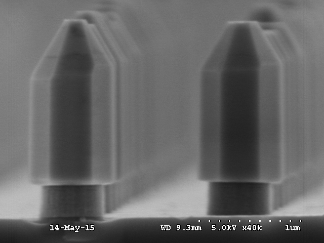
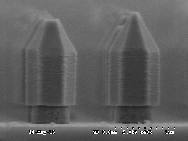
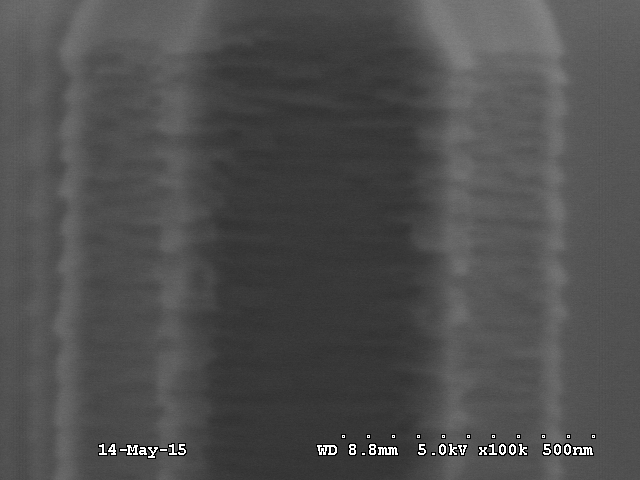
Figure1a_SEM … cross-section.bmp
image/x-ms-bmp (308kB)
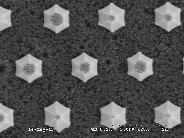
Figure1a_inset … plan-view.bmp
image/x-ms-bmp (308kB)
Figure1b_SEM … cross-section.bmp
image/x-ms-bmp (308kB)
Figure1b_inset … plan-view.bmp
image/x-ms-bmp (308kB)
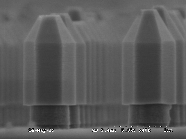
Figure1c_SEM … cross-section.bmp
image/x-ms-bmp (308kB)
Figure1c_inset … plan-view.bmp
image/x-ms-bmp (308kB)
Figure1d_SEM … cross-section.bmp
image/x-ms-bmp (308kB)
Figure1e_SEM … cross-section.bmp
image/x-ms-bmp (308kB)
Figure1f_SEM … cross-section.bmp
image/x-ms-bmp (308kB)
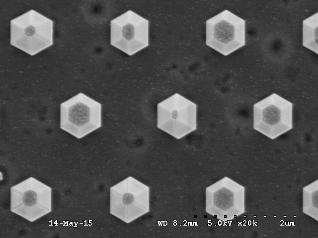
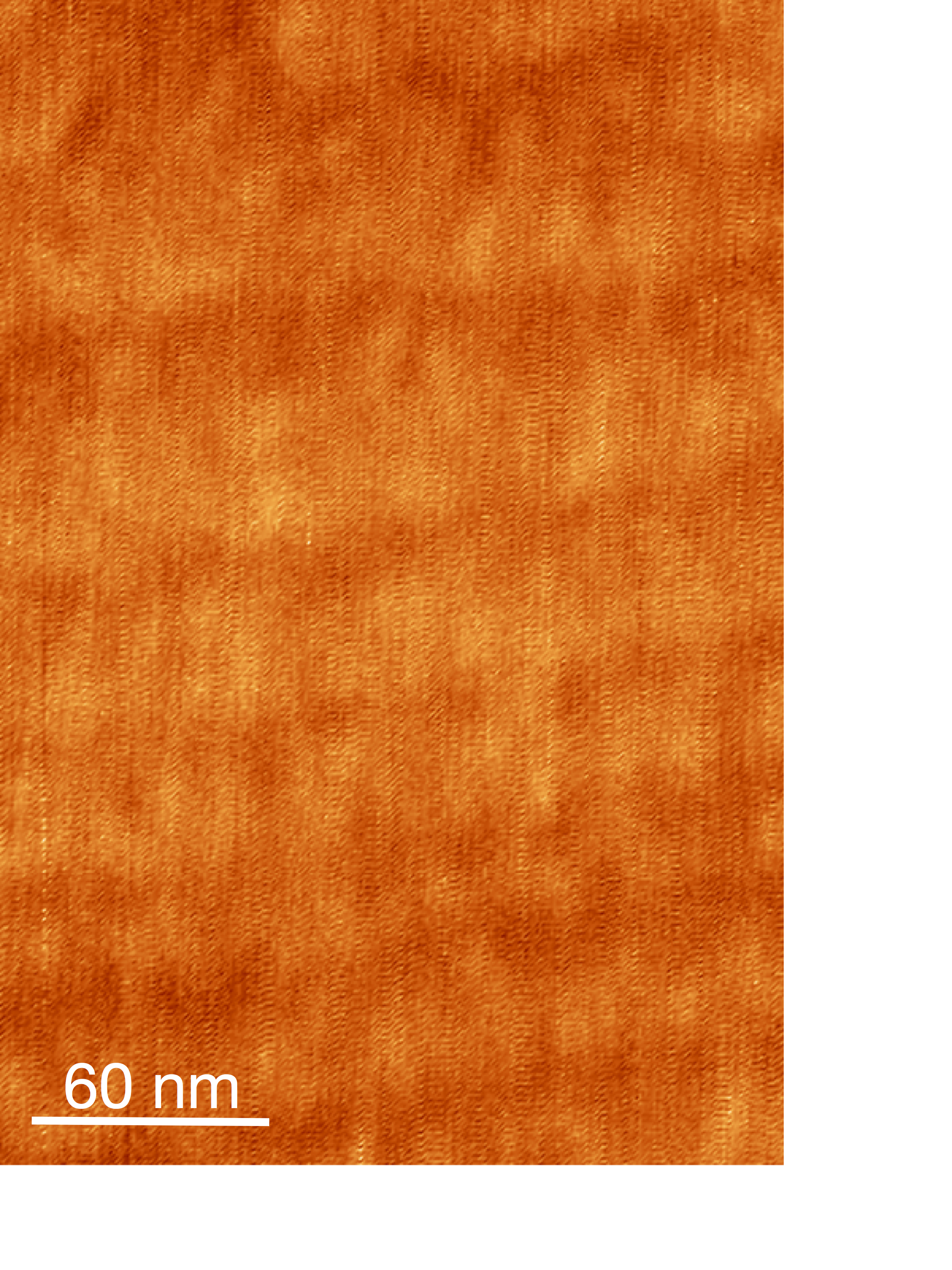
Figure2a_AFM_GaN.png
image/png (8MB)
Figure2a_AFM_GaN.txt
text/plain (2MB)
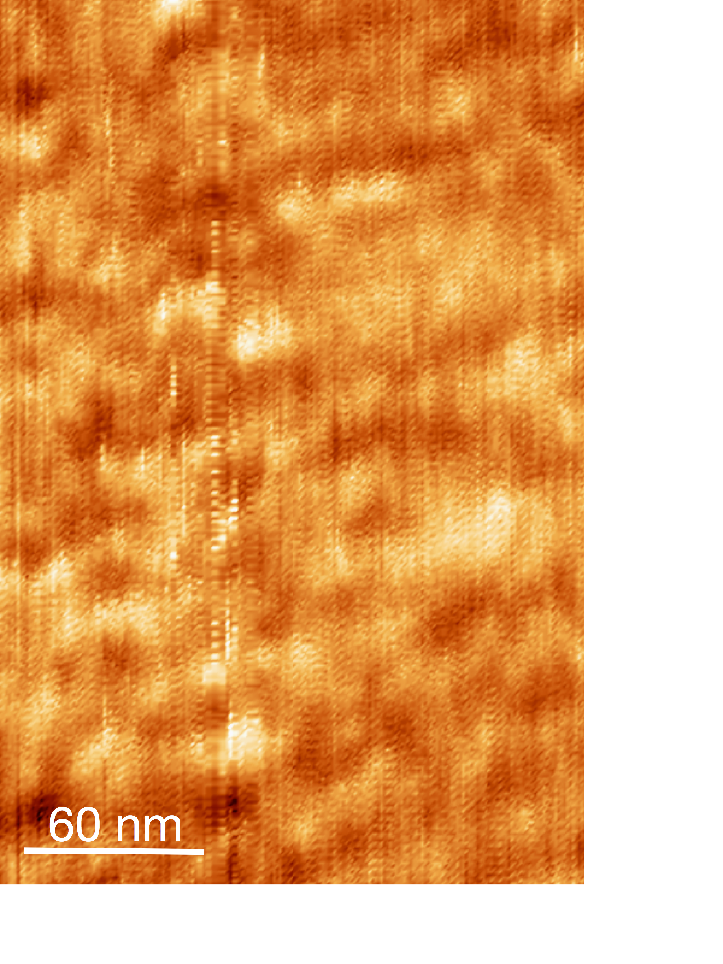
Figure2b_AFM_2minInGaN.png
image/png (7MB)
Figure2b_AFM_2minInGaN.txt
text/plain (1MB)
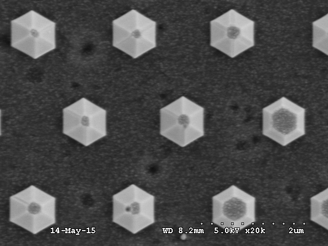
Figure2c_AFM_6minInGaN.png
image/png (5MB)
Figure2c_AFM_6minInGaN.txt
text/plain (1MB)
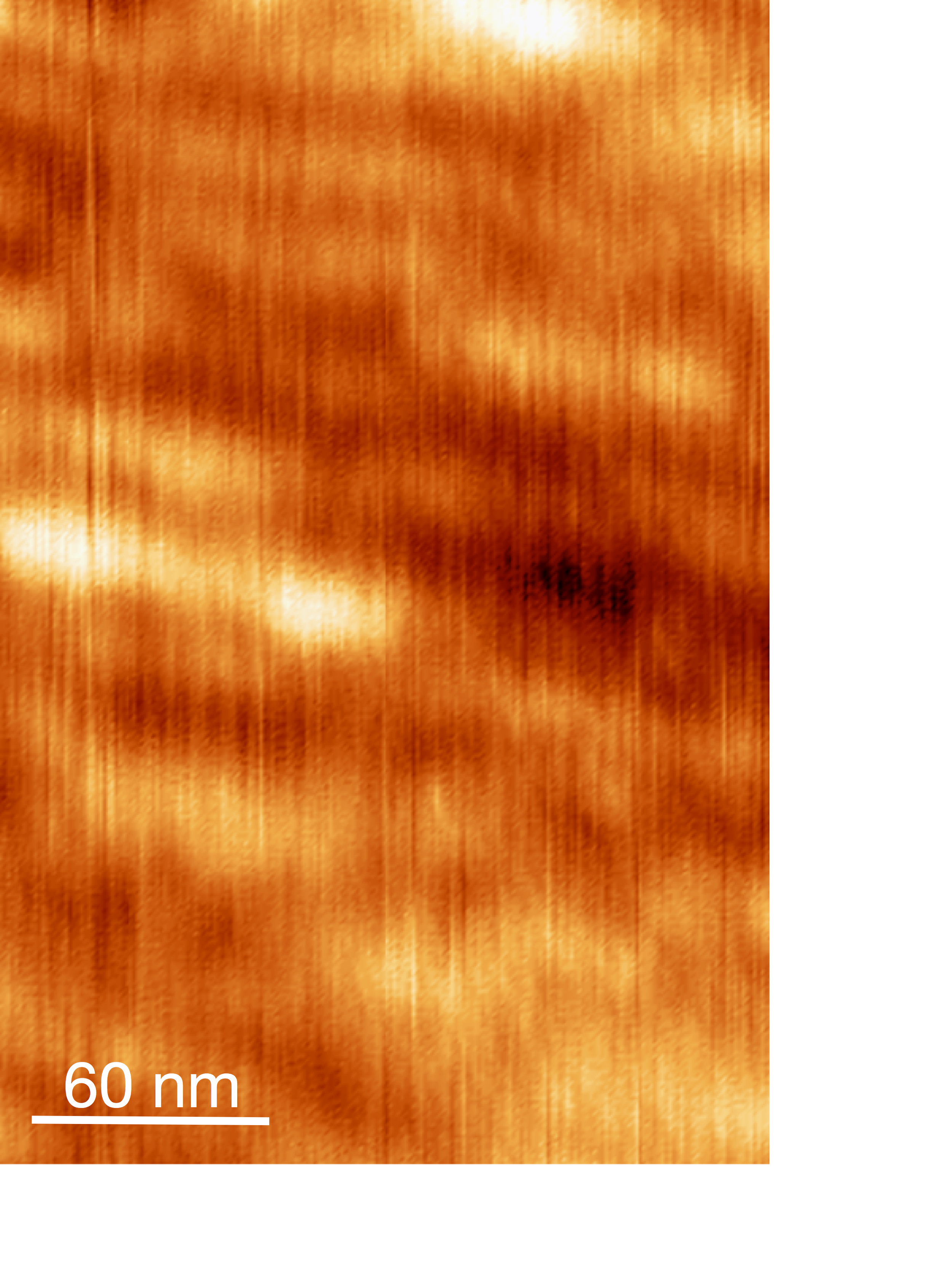
Figure2d_AFM_18minInGaN.png
image/png (5MB)
Figure2d_AFM_18minInGaN.txt
text/plain (1MB)
Figure2e_AFM … growth_time.xlsx
application/vnd.openxmlformats-officedocument.spreadsheetml.sheet (68kB)
Figure2f_AFM … and_edges.xlsx
application/vnd.openxmlformats-officedocument.spreadsheetml.sheet (53kB)
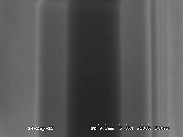
Figure3a_TEM_2minInGaN.tif
image/tiff (1MB)
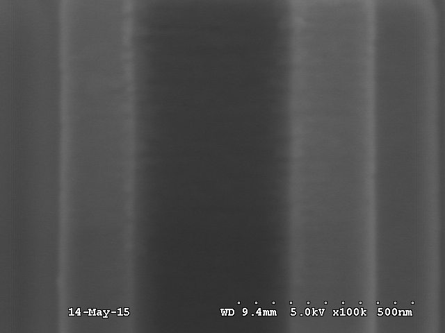
Figure3b_TEM_6minInGaN.tif
image/tiff (1MB)
Figure3c_TEM_18minInGaN.tif
image/tiff (1MB)
Figure3d_TEM … nInGaNuncapped.tif
image/tiff (1MB)
Figure3e_HRTEM_atomic_step.tif
image/tiff (277kB)
Figure4a_EDX_2minInGaN.xlsx
application/vnd.openxmlformats-officedocument.spreadsheetml.sheet (21kB)
Figure4b_EDX_6minInGaN.xlsx
application/vnd.openxmlformats-officedocument.spreadsheetml.sheet (19kB)
Figure4c_EDX_18minInGaN.xlsx
application/vnd.openxmlformats-officedocument.spreadsheetml.sheet (29kB)
Figure4d_EDX_18minInGaNuncapped.xlsx
application/vnd.openxmlformats-officedocument.spreadsheetml.sheet (29kB)
Figure5_depth_CL.xlsx
application/vnd.openxmlformats-officedocument.spreadsheetml.sheet (3MB)
Creators
Pierre-Marie Coulon
University of Bath
Contributors
Shahrzad Hosseini-Vajargah
Researcher
University of Cambridge
An Bao
Contributor
University of Cambridge
Emmanuel Le Boulbar
Researcher
University of Bath
Ionut Girgel
Contributor
University of Bath
Colin J. Humphreys
Contributor
University of Cambridge
Rachel Oliver
Contributor
University of Cambridge
Duncan Allsopp
Project Member
University of Bath
Philip Shields
Project Leader
University of Bath
University of Bath
Rights Holder
Documentation
Data collection method:
Secondary electron images were captured using a Hitachi S-4300 scanning electron microscope (SEM). An accelerating voltage of 5 kV was used to collect the images. Tapping mode was used for all the AFM measurements. The low magnification TEM investigations were performed using a FEI Tecnai Osiris fitted with high brightness field emission gun (XFEG). Experiments were carried out at an accelerating voltage of 200 kV, and a beam current of 0.5 nA. The HRTEM observations were performed using a FEI Titan3 Themis 300 fitted with high brightness field emission gun (XFEG) with S-TWIN objective lens and monochromator (energy spread approx. 0.25 eV). Energy dispersive X-Ray spectroscopy analyses were carried out using an FEI Tecnai Osiris TEM. This microscope was equipped with XFEG and Super X system EDX detectors. This detector comprises 4 Bruker silicon drift detectors (SDD) arranged symmetrically around the optic axis of the microscope for high collection efficiency and high count rate. Spectrum images were acquired at a spatial sampling of 2 nm/pixel or 4 nm/pixel and 200 ms/pixel dwell times with a probe current of approximately 0.5 nA, at an accelerating voltage of 200 kV. Cathodoluminescence spectroscopy was carried out at room temperature in a modified FEI Quanta 250 field emission SEM with various accelerating voltages. Light was collected using an NA0.28 reflecting objective with its axis perpendicular to the electron beam and focused directly to the entrance of the spectrograph using an off-axis paraboloidal mirror. We used a 125 mm focal length spectrograph with a 600 lines/mm grating and 50 μm entrance slit, coupled to a cooled electron multiplying charge-coupled device (EMCCD) detector.
Data processing and preparation activities:
The as-grown GaN and GaN/InGaN NRs samples were mechanically removed from the Si substrate and dispersed on a host Si substrate. The NRs were then carefully located within a SEM prior to AFM measurements to ensure that the studied NRs were lying flat on the substrate. Line flattening on the selected areas of interest was performed to obtain the AFM height image of the m-plane facet for the GaN faceted NRs and the three uncapped InGaN samples. The RMS roughness value for each sample was extracted from the center of the m-facet to avoid any contribution of the apices.The images to calculate RMS roughnesses are the same size and have all undergone line flattening. The height and periodicity of the features or striations were extracted via AFM line scans traced along the c-axis. The miscut calculation was performed on the GaN faceted NR.The profile was extracted using a Y average filter, providing the average step height and the average step width values.The miscut angle was calculated by the following equation using the theoretical value of the monolayer step height: MiscutAngle=arctan((average step height)/(average step width)). The samples for TEM observations and EDX measurements were prepared by a tripod polishing method using an Allied Tech Multiprep unit. Specimens were then ion-milled with a Gatan Precision Ion Polishing System (PIPS) using 1.5–5 keV argon ions for further thinning and removing the residue of polishing contamination from the specimens. Samples for HRTEM were prepared by a dual beam focused ion beam milling using a FEI Nova 200 NanoLab high resolution Field Emission Gun Scanning Electron Microscope (FEGSEM) with precise Focused Ion Beam (FIB) etch and deposition capabilities. The nanorods were protected by a platinum layer prior to etching to reduce the damage that could occur with the use of an ion beam system. Using principal component analysis (PCA) and independent component analysis (ICA) (implemented in HyperSpy47), two independent and uncorrelated components were identified in the spectrum images. The first component contains Ga and N X-ray peaks and the second component contain Ga, In, and N X-ray peaks. To obtain the composition of the InGaN shell, the intensities of Ga Kα and In Lα peaks were quantified using the Cliff-Lorimer method and the k-factor provided by the manufacturer of the EDX system (Bruker). The errors were also estimated from Poisson statistics. The ICA technique is capable of differentiating true spectra from the underlying noise efficiently and, as a result, noisy spectra can be tolerated. Using the ICA technique, the required sample beam dose was therefore significantly minimized without compromising the accuracy of quantification.
Funders
Engineering and Physical Sciences Research Council
https://doi.org/10.13039/501100000266
Lighting the Future
EP/I012591/1
Engineering and Physical Sciences Research Council
https://doi.org/10.13039/501100000266
Manufacturing of Nano-Engineered III-Nitride Semiconductors
EP/M015181/1
Engineering and Physical Sciences Research Council
https://doi.org/10.13039/501100000266
Free-Standing Wurzite AIGaN Subsrates for Deep Ultraviolet Devices
EP/K008323/1
Publication details
Publication date: 2016
by: University of Bath
Version: 1
DOI: https://doi.org/10.15125/BATH-00224
URL for this record: https://researchdata.bath.ac.uk/224
Related papers and books
Coulon, P.-M., Vajargah, S. hosseini, Bao, A., Edwards, P. R., Le Boulbar, E. D., Girgel, I., Martin, R. W., Humphreys, C. J., Oliver, R. A., Allsopp, D. W. E., and Shields, P. A., 2017. Evolution of the m-Plane Quantum Well Morphology and Composition within a GaN/InGaN Core–Shell Structure. Crystal Growth & Design, 17(2), 474-482. Available from: https://doi.org/10.1021/acs.cgd.6b01281.
Contact information
Please contact the Research Data Service in the first instance for all matters concerning this item.
Contact person: Pierre-Marie Coulon
Faculty of Engineering & Design
Electronic & Electrical Engineering
