Dataset for "Optical properties and resonant cavity modes in axial InGaN/GaN nanotube microcavities"
This dataset contains scanning electron microscopy (SEM) images, Catodoluminescence (CL), MicroPL and Confocal PL measurements and Finite-Difference Time-Domain (FDTD) simulations carried out on InGaN/GaN nanotube microcavities. The samples were fabricated via a combination of Displacement Talbot Lithography for patterning and inductively coupled plasma top-down dry-etching. SEM imaging were used to assess first, the patterning of SiNx mask, and second, the InGaN/GaN nanotube morphology and dimensions. CL were used to assess the optical properties of individual InGaN/GaN nanotube. MicroPL and Confocal PL were used to carry out continuous excitation at room temperature of isolated InGaN/GaN nanotube. FDTD simulations were used to investigate the nature of the resonant modes. Correlation between PL techniques and FDTD simulation suggests that both mixed whispering gallery – Fabry-Perot cavity modes are observed within the single nanotube.
Cite this dataset as:
Coulon, P.,
Pugh, J.,
Athanasiou, M.,
Kusch, G.,
Le Boulbar, E.,
2017.
Dataset for "Optical properties and resonant cavity modes in axial InGaN/GaN nanotube microcavities".
Bath: University of Bath Research Data Archive.
Available from: https://doi.org/10.15125/BATH-00414.
Export
Data
Fig1.a_SEM_10k_plan-view.tif
image/tiff (194kB)
Creative Commons: Attribution 4.0
SEM plan-view image of the resist mask after DTL exposure for a dose of 100 mJ/cm2
Fig1.b_SEM_10k_plan-view.tif
image/tiff (223kB)
Creative Commons: Attribution 4.0
SEM plan-view image of the resist mask after DTL exposure for a dose of 200 mJ/cm2
Fig1.c_SEM_10k_plan-view.tif
image/tiff (232kB)
Creative Commons: Attribution 4.0
SEM plan-view image of the resist mask after DTL exposure for a dose of 480 mJ/cm2
Fig2.a_SEM … cross-section.bmp
image/x-ms-bmp (308kB)
Creative Commons: Attribution 4.0
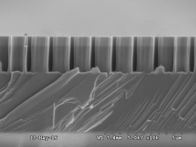
SEM low magnification cross-section image of the axial InGaN/GaN nanotube LED structures obtained after DTL patterning and ICP top-down etching
Fig2.b_SEM … cross-section.bmp
image/x-ms-bmp (308kB)
Creative Commons: Attribution 4.0
SEM high magnification cross-section image of the axial InGaN/GaN nanotube LED structures obtained after DTL patterning and ICP top-down etching
Inset_Fig2.b … plan-view.bmp
image/x-ms-bmp (308kB)
Creative Commons: Attribution 4.0
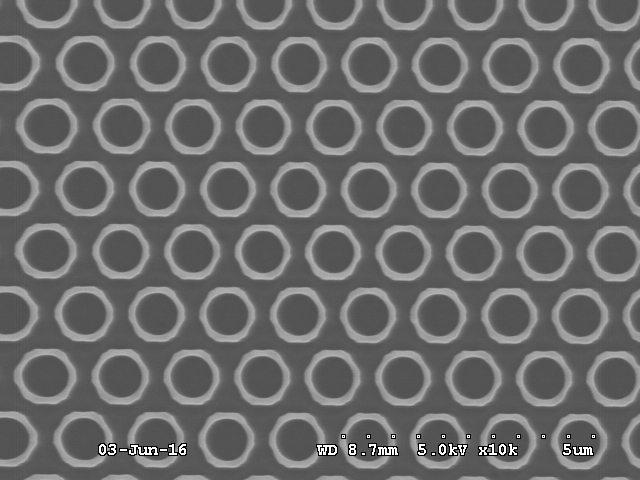
SEM plan-view image of the axial InGaN/GaN nanotube LED structures obtained after DTL patterning and ICP top-down etching
Fig3.a_SEM_24k_tilt-view.tif
image/tiff (976kB)
Creative Commons: Attribution 4.0
SEM tilt-view image of the axial InGaN/GaN nanotube LED structures obtained after DTL patterning and ICP top-down etching
Fig3.d_CL_spectra.xlsx
application/vnd.openxmlformats-officedocument.spreadsheetml.sheet (77kB)
Creative Commons: Attribution 4.0
CL spectra extracted from the hyperspectral dataset at SQW positions for various InGaN/GaN nanotubes
Fig4.a_SEM_30k.bmp
image/x-ms-bmp (308kB)
Creative Commons: Attribution 4.0
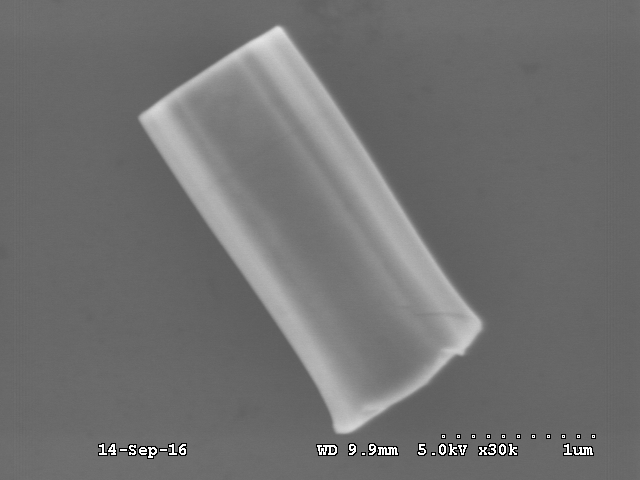
SEM images of a single dispersed InGaN/GaN nanotube
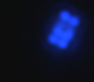
Fig4.b_41kw_cm-2.png
image/png (146kB)
Creative Commons: Attribution 4.0
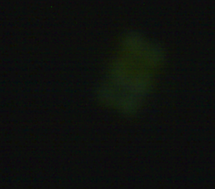
CCD images of a single InGaN/GaN nanotube pumped with µPL at 41 kW/cm2
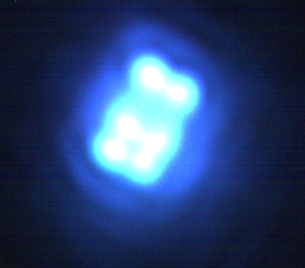
Fig4.c_205kw_cm-2.png
image/png (151kB)
Creative Commons: Attribution 4.0
CCD images of a single InGaN/GaN nanotube pumped with µPL at 205 kW/cm2
Fig4.d_410_kw_cm-2.png
image/png (211kB)
Creative Commons: Attribution 4.0
CCD images of a single InGaN/GaN nanotube pumped with µPL at 410 kW/cm2
Fig4.e_and … measurments.xlsx
application/vnd.openxmlformats-officedocument.spreadsheetml.sheet (728kB)
Creative Commons: Attribution 4.0
InGaN/GaN nanotube spectra for a continuous CW 375 nm excitation at RT with (e) µPL and (f) confocal microscope technique.
Fig5.a_FDTD_spectra.xlsx
application/vnd.openxmlformats-officedocument.spreadsheetml.sheet (1MB)
Creative Commons: Attribution 4.0
Normalized E-field intensity spectra of a 2.4 µm tall InGaN/GaN nanotube with a circular and non-circular shape
Fig7_Comparison … with_FDTD.xlsx
application/vnd.openxmlformats-officedocument.spreadsheetml.sheet (226kB)
Creative Commons: Attribution 4.0
Comparison between the normalized simulated field intensity spectra and the normalized spectra for the employed CL/PL techniques.
Fig8.a_FDTD … variation.xlsx
application/vnd.openxmlformats-officedocument.spreadsheetml.sheet (2MB)
Creative Commons: Attribution 4.0
E-field intensity spectra of a 2.4 µm, 1.6 and 700 nm tall InGaN/GaN nanotube with a SQW 600nm bellow
Fig8.b_FDTD … variation.xlsx
application/vnd.openxmlformats-officedocument.spreadsheetml.sheet (2MB)
Creative Commons: Attribution 4.0
E-field intensity spectra of a 2.4 µm tall InGaN/GaN nanotube with a SQW changing from the center of the nanotube at 1220 nm to the actual experimental position of the SQW at 1820 nm.
Fig3.b-c_CLmap.zip
application/zip (32MB)
Creative Commons: Attribution 4.0
Fig5.b_FDTD_E-field_snapshot.txt
text/plain (700kB)
Creative Commons: Attribution 4.0
Fig5.c_FDTD_E-field_snapshot.txt
text/plain (700kB)
Creative Commons: Attribution 4.0
Fig6.a_FDTD_E-field_snapshot.txt
text/plain (1MB)
Creative Commons: Attribution 4.0
Fig6.b_FDTD_E-field_snapshot.txt
text/plain (1MB)
Creative Commons: Attribution 4.0
Fig6.c_FDTD_E-field_snapshot.txt
text/plain (1MB)
Creative Commons: Attribution 4.0
Fig6.d_FDTD_E-field_snapshot.txt
text/plain (1MB)
Creative Commons: Attribution 4.0
Fig6.e_FDTD_E-field_snapshot.txt
text/plain (1MB)
Creative Commons: Attribution 4.0
Fig6.f_FDTD_E-field_snapshot.txt
text/plain (1MB)
Creative Commons: Attribution 4.0
Fig6.g_FDTD_E-field_snapshot.txt
text/plain (1MB)
Creative Commons: Attribution 4.0
Fig6.h_FDTD_E-field_snapshot.txt
text/plain (1MB)
Creative Commons: Attribution 4.0
All items available for download under a Creative Commons Attribution (CC-BY) licence.
Creators
Pierre-Marie Coulon
University of Bath
Jon Pugh
Contributor
University of Bristol
Modestos Athanasiou
Contributor
University of Sheffield
Gunnar Kusch
Contributor
University of Strathclyde
Emmanuel Le Boulbar
Contributor
University of Bath
Contributors
Andrei Sarua
Contributor
University of Bristol
Rick Smith
Contributor
University of Sheffield
Robert Martin
Contributor
University of Strathclyde
Tao Wang
Contributor
University of Sheffield
Martin Cryan
Contributor
University of Bristol
Duncan Allsopp
Contributor
University of Bath
Philip Shields
Project Leader
University of Bath
University of Bath
Rights Holder
Documentation
Data collection method:
Secondary electron images were captured using a Hitachi S-4300 scanning electron microscope (SEM). An accelerating voltage of 5 kV was used to collect the images. Cathodoluminescence hyperspectral imaging measurements were carried out at room temperature in a modified FEI Quanta 250 field emission SEM using electron energies of 5.0 keV and beam currents of approximately 1 nA. Light was collected using an NA 0.28 reflecting objective with its axis perpendicular to the electron beam and focused directly on the entrance of the spectrograph using an off-axis paraboloidal mirror. We used a 125 mm focal length spectrograph with a 600 lines/mm grating and 50 μm entrance slit, coupled to a cooled electron multiplying charge-coupled device (EMCCD) detector. µPL characterization was carried out on single nanotube cavities in an in-house made micro-PL system. A 375 nm continuous wave (CW) laser diode was used to selectively excite the InGaN/GaN SQW. A 50x magnification, 0.43 NA objective was used to focus the excitation laser down to ~ 2μm and collect the emission through a 1 mm fibre bundle. A 0.55 m Jobin Yvon spectrometer (iHR550) was used to disperse the emission and the emission was detected with an air-cooled charge coupled device (CCD). The system was equipped with X-Y-Z motorized stages allowing to selectively excite single nanotubes. All the measurements were performed at room temperature. Confocal PL characterization was performed using a commercial WITec confocal microscope. A 375 nm continuous wave (CW) diode laser was used as an optical pumping source and the system was equipped with a 300 mm Princeton instruments monochromator (SP2300i) and an air-cooled charge coupled device (CCD). An objective lens (100×, NA=0.95) was used to focus the laser beam down to a spot with a diameter of ~400 nm. The emission was dispersed by the monochromator with a resolution of ~0.1 nm. An optical fiber with a diameter of 10 µm acted as a pinhole, thus allowing the emission to be collected from only where the sample was excited. The system was equipped with a high-resolution x-y-z piezo-stage to individually address and examine single nanotubes. The spatial resolution of the system was ~ 160 nm. All the measurements were performed at room temperature. A three-dimensional finite difference time domain (FDTD) approach has been used to simulate the nanotube structure using commercial-grade software [Lumerical Solutions, Inc. http://www.lumerical.com/tcad-products/fdtd/]. A dipole source with emission wavelengths from 370 to 720 nm was vertically positioned in the plane of the nanotube quantum wells and centred within the width of the walls. All the geometrical data used for the simulation are from the SEM measurement of our nanotube. The n-GaN, p-GaN and GaN-substrate layers are given a refractive index defined by ellipsometry measurements performed on the as-grown structure at the University of Strathclyde. The InGaN quantum well layer is 3nm thick (n=2.6). There is a minimum of fifteen mesh cells per wavelength in the simulation that is run for 2000fs. Frequency-domain power monitors have been used to record the emission profile over the simulation region, which is surrounded by perfectly matched layer absorbing boundaries on all sides. The simulated spectra are collected by a grid of 12 time-monitors placed at various points inside the nanotube structure, accurately calculating the envelope of the time-domain field signal. For the perfectly-circular higher-Q examples, each resonant peak is isolated in the frequency domain using a Gaussian filter, and by taking the inverse Fourier transforms the time decay have been calculated separately for each peak. The slope of the time decay is used to calculate the Q-factor of each resonance. In the DTL fabricated structures, the electromagnetic fields decay completely from the simulation in a time that can be simulated reasonably by FDTD. Therefore, the resonant frequencies are found from the time-monitors along with the full-width half-maximum (FWHM) of the corresponding peaks. We can then use Q=fR/Δf where fR is the resonant frequency and Δf is the FWHM.
Data processing and preparation activities:
The nanotube investigated by µPL and Confocal PL were mechanically removed from the substrate in an ultrasonic bath and then dispersed on a host sapphire substrate
Funders
Engineering and Physical Sciences Research Council
https://doi.org/10.13039/501100000266
Manufacturing of Nano-Engineered III-Nitride Semiconductors
EP/M015181/1
Publication details
Publication date: 2017
by: University of Bath
Version: 1
DOI: https://doi.org/10.15125/BATH-00414
URL for this record: https://researchdata.bath.ac.uk/414
Related papers and books
Coulon, P. -M., Pugh, J. R., Athanasiou, M., Kusch, G., Le Boulbar, E. D., Sarua, A., Smith, R., Martin, R. W., Wang, T., Cryan, M., Allsopp, D. W. E., and Shields, P. A., 2017. Optical properties and resonant cavity modes in axial InGaN/GaN nanotube microcavities. Optics Express, 25(23), 28246. Available from: https://doi.org/10.1364/oe.25.028246.
Contact information
Please contact the Research Data Service in the first instance for all matters concerning this item.
Contact person: Pierre-Marie Coulon
Faculty of Engineering & Design
Electronic & Electrical Engineering
