Fabrication of high-aspect ratio GaN nanostructures for advanced photonic devices
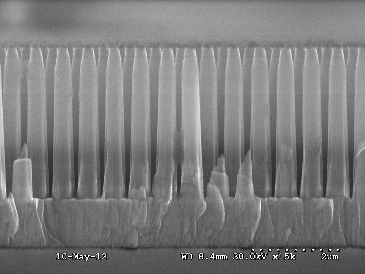
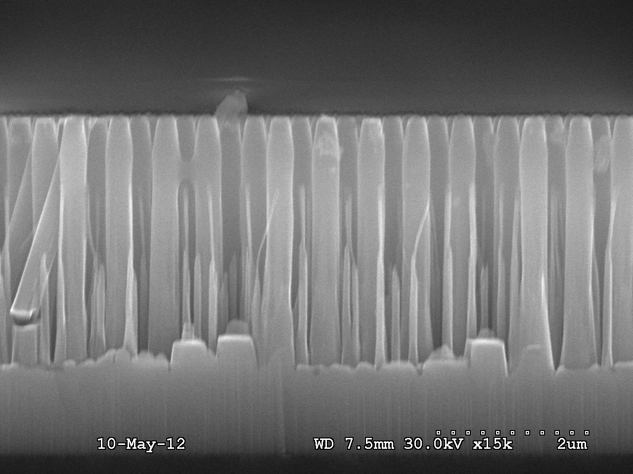
The ability to manipulate and guide light is crucial for the fabrication of photonic circuit. The behaviour of the light within a nanostructure is complex and manipulating light often require to accurately tune the dimension and the shape of the nanostructure. Semiconducting material such as Gallium Nitride (GaN) nanostructures could be used as building blocks to fabricate active and passive components for photonic circuit, such has core-shell light emitting diode and non-linear photonic-diode. Understanding the top-down fabrication process and controlling the profile of nanostructures is crucial to achieve and design appropriate devices characteristics. We investigated the impact of the temperature and the pressure on the profile of Inductively Coupled Plasma (ICP) etched Gallium Nitride nanorods and nanopores arrays. The nanostructure arrays were characterized via Secondary Electron Microscopy. We used the Secondary Electron images collected to extract the dimensions of the etched nanorods and nanopores. Our results show a threshold in the etch behaviour at a temperature of 125°C, which greatly enhanced the verticality of the GaN nanorods, whilst the modification of the pressure enables a fine tuning of the nanorod profile.
This dataset is the result of an investigation into the impact of the temperature and pressure on the fabrication of Gallium Nitride nanostructures. The dataset contains data acquired from etched nanorods and nanopores.The data was acquired using a Hitachi S-4300 scanning electron microscope (SEM). The secondary electron (SE) images were produced using the manufacturer-supplied software. Figure numbers in the data file descriptions refer to the Microelectronic Engineering article by Le Boulbar et al. (2016) referenced in the related publications section.
Cite this dataset as:
Le Boulbar, E.,
Lewins, C.,
Allsopp, D.,
Bowen, C.,
Shields, P.,
2016.
Fabrication of high-aspect ratio GaN nanostructures for advanced photonic devices.
Bath: University of Bath Research Data Archive.
Available from: https://doi.org/10.15125/BATH-00154.
Export
Data
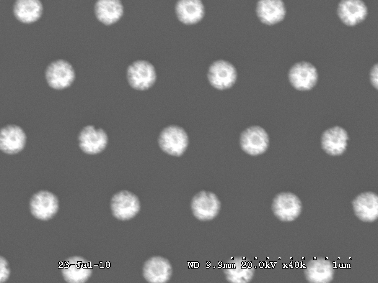
Nanodots_metal_mask.bmp
image/x-ms-bmp (1MB)
Creative Commons: Attribution 4.0
SE image used in Fig. 1a
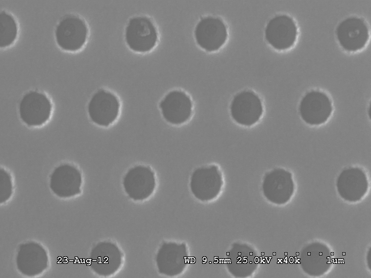
Nanoholes_metal_mask.bmp
image/x-ms-bmp (1MB)
Creative Commons: Attribution 4.0
SE image used in Fig. 1b
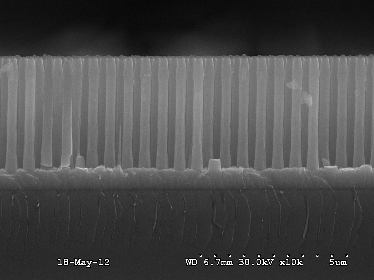
NR_600nmpitch_75deg.bmp
image/x-ms-bmp (1MB)
Creative Commons: Attribution 4.0
SE image used in Fig. 2a
NR_600nmpitch_100deg.bmp
image/x-ms-bmp (1MB)
Creative Commons: Attribution 4.0
SE image used in Fig. 2b
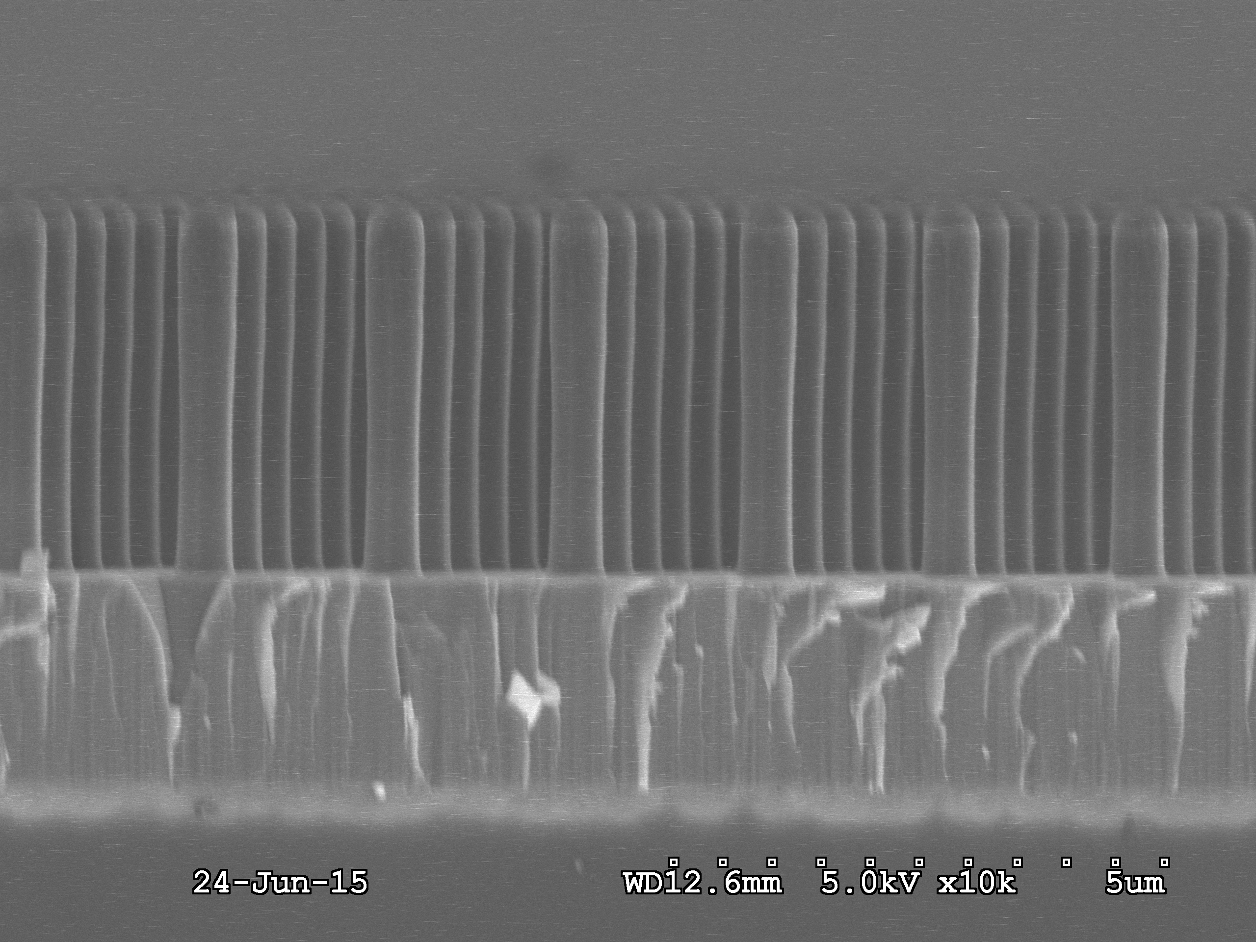
NR_600nmpitch_150deg.bmp
image/x-ms-bmp (1MB)
Creative Commons: Attribution 4.0
SE image used in Fig. 2c
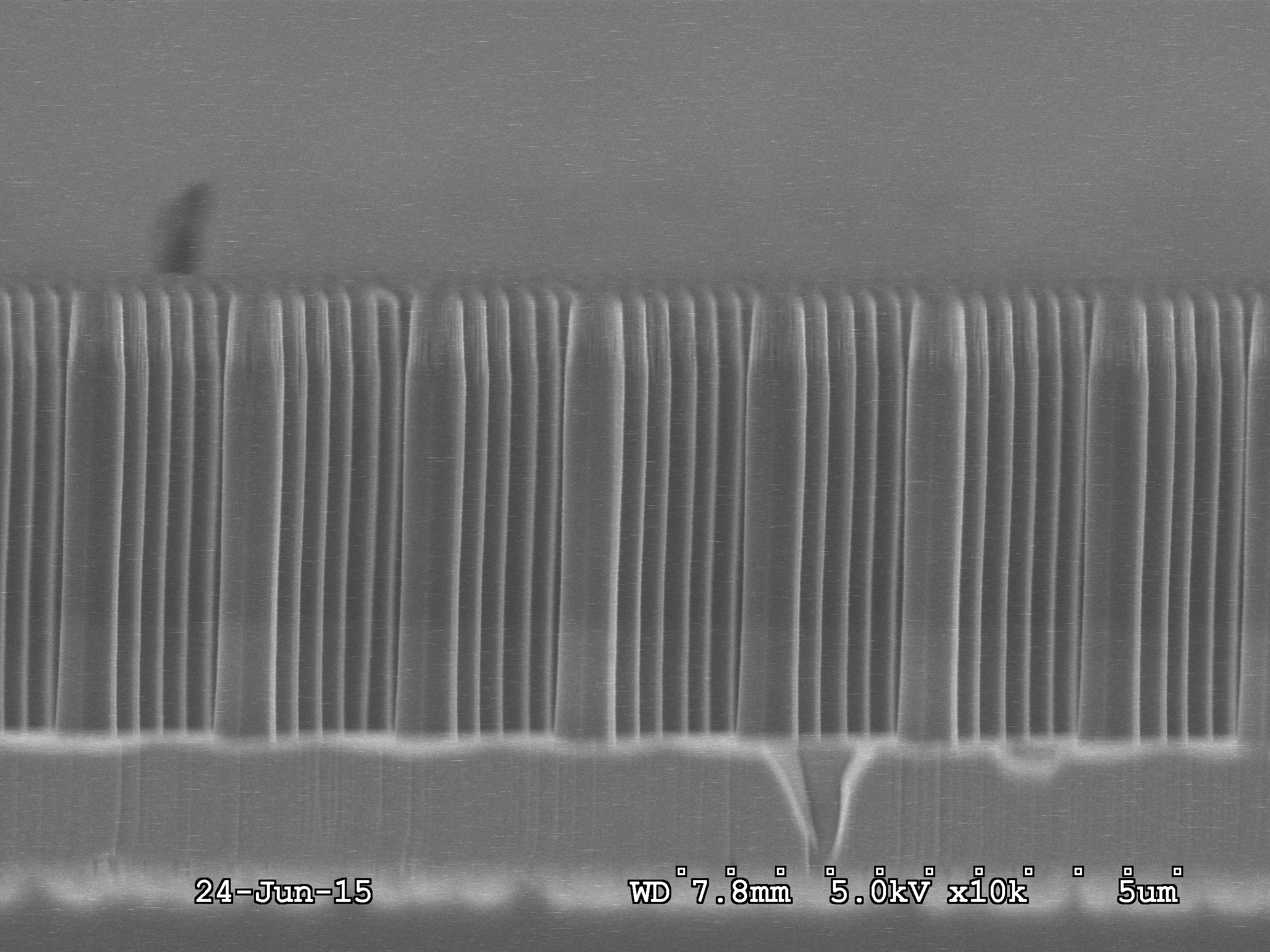
NR_600nmpitch_175deg.bmp
image/x-ms-bmp (4MB)
Creative Commons: Attribution 4.0
SE image used in Fig. 2d
Fig3_dataset.xlsx
application/vnd.openxmlformats-officedocument.spreadsheetml.sheet (10kB)
Creative Commons: Attribution 4.0
Data used to create Fig. 3
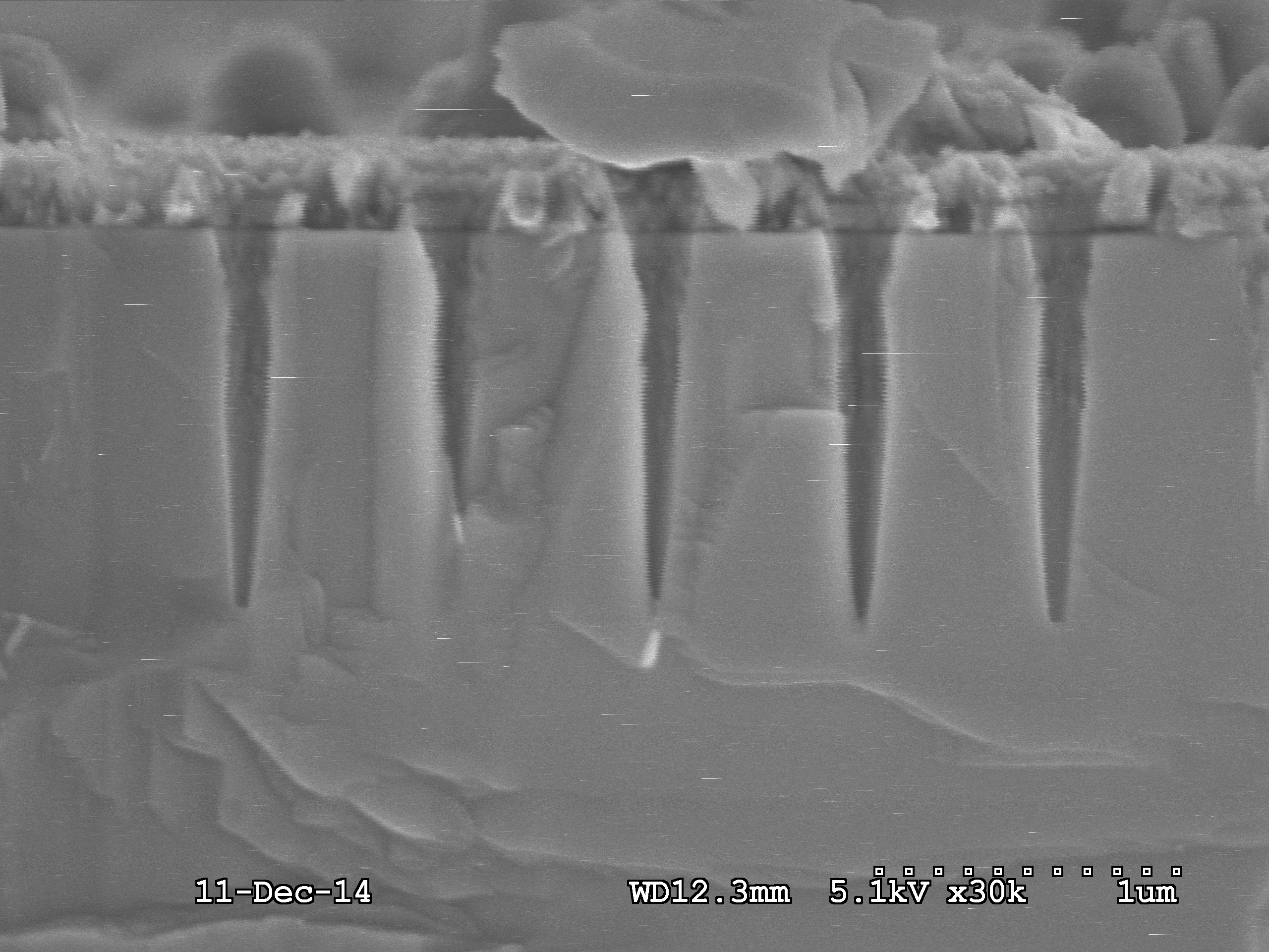
2micronpitch … 120RF_800ICP.bmp
image/x-ms-bmp (4MB)
Creative Commons: Attribution 4.0
SE image used in Fig. 3a
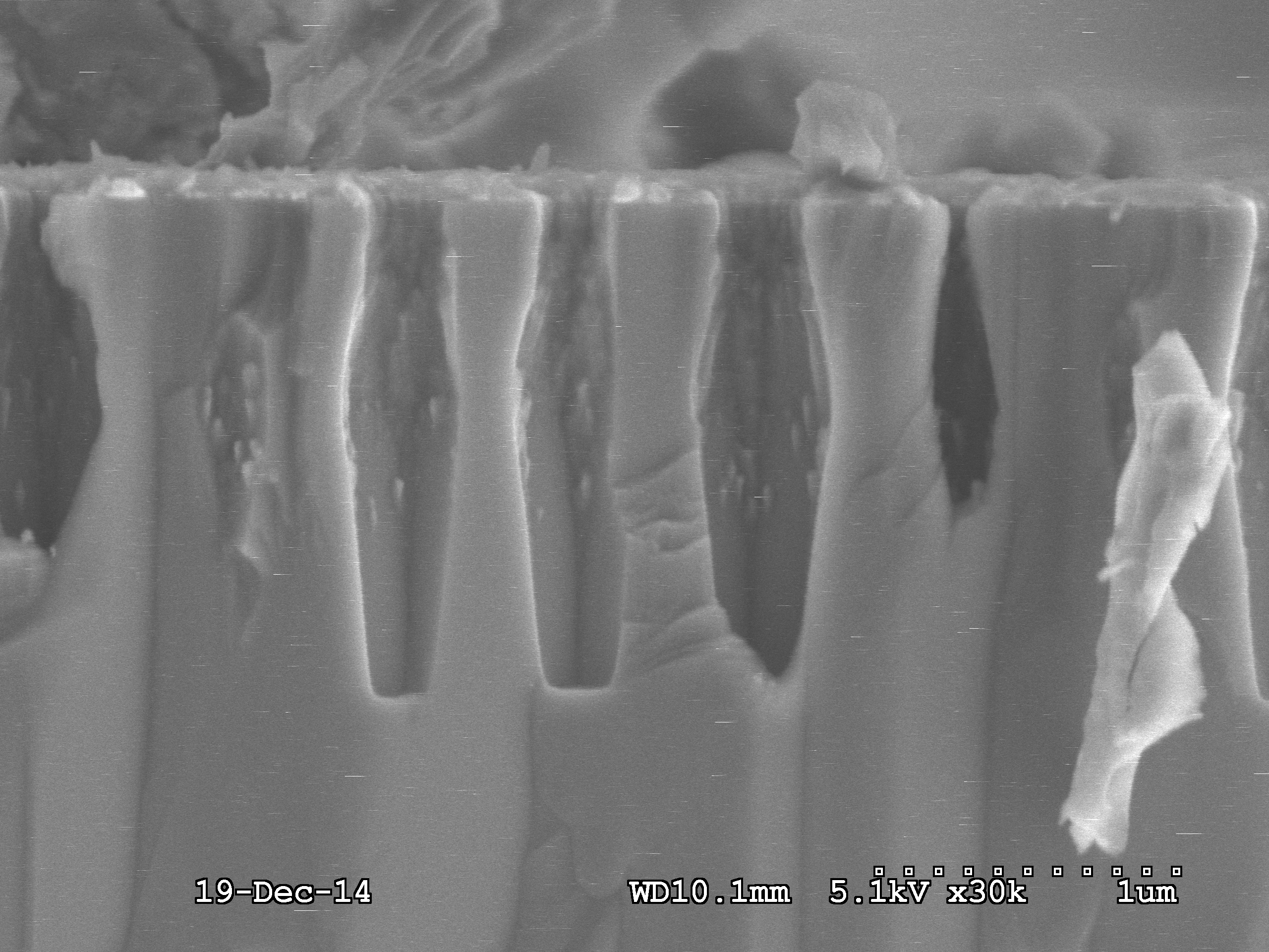
2micronptich … 120RF_800ICP.bmp
image/x-ms-bmp (4MB)
SE image used in Fig. 4b
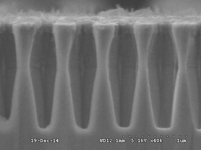
2micronptich … 120RF_800ICP.bmp
image/x-ms-bmp (4MB)
SE image used in Fig. 4c
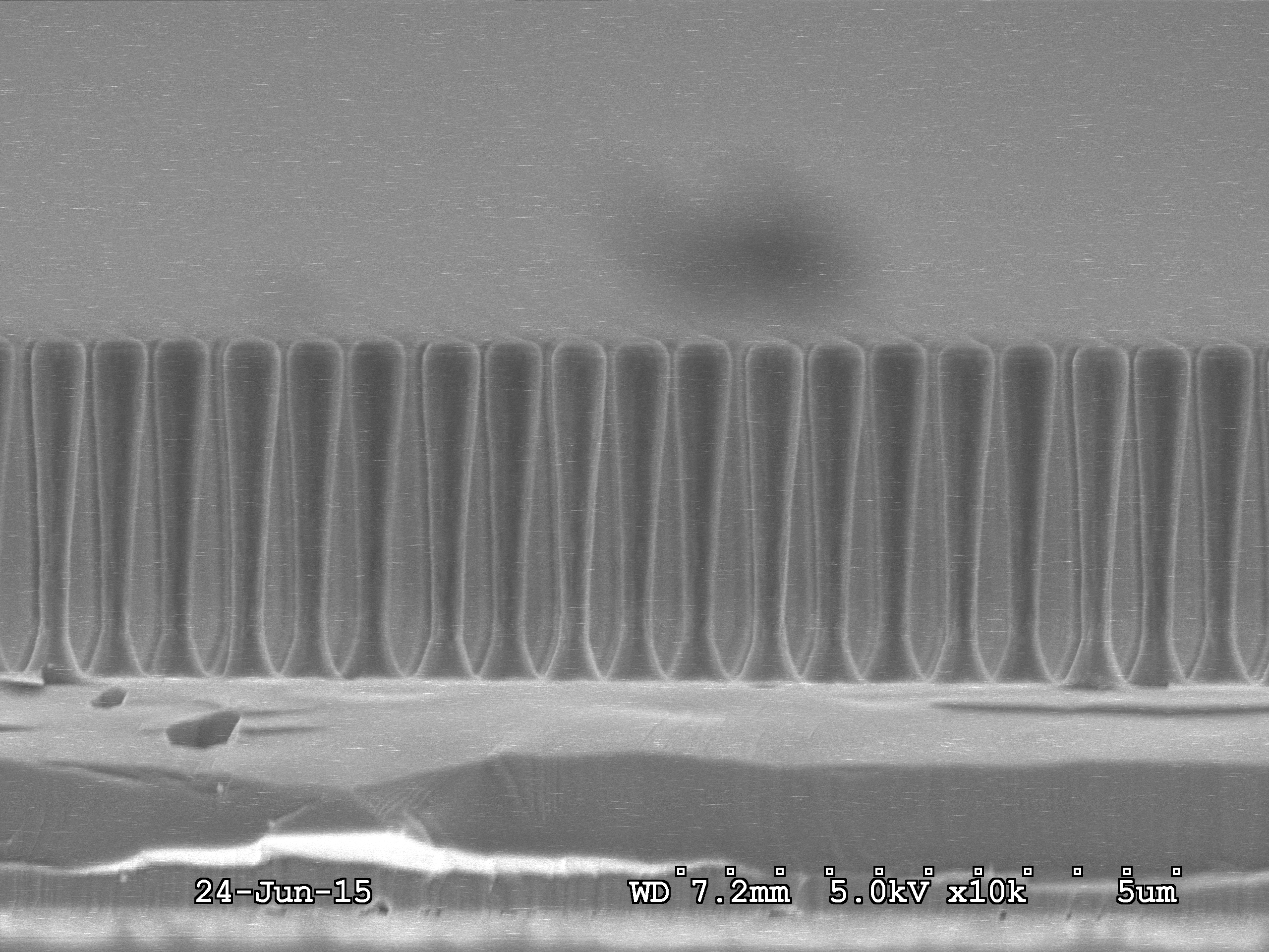
NP_600nm_200deg_5min_15mT.bmp
image/x-ms-bmp (4MB)
NP_600nm_250deg_5min_15mT.bmp
image/x-ms-bmp (4MB)
SE image used in Fig. 5b
NP_600nm_350deg_5min_15mT.bmp
image/x-ms-bmp (308kB)
SE image used in Fig. 5b
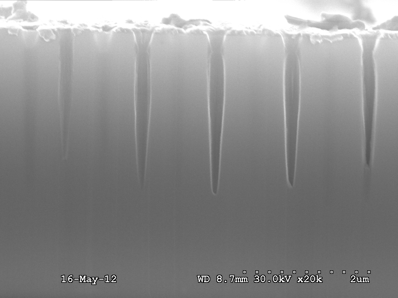
Deep_NP_150deg_30min_15mT.bmp
image/x-ms-bmp (1MB)
SE image used in Fig. 6a
Fig7_Raw_data_Aspect_ratio.xlsx
application/vnd.openxmlformats-officedocument.spreadsheetml.sheet (8kB)
Creative Commons: Attribution 4.0
Data used in Fig. 7
Creators
Emmanuel Le Boulbar
University of Bath
Christopher Lewins
Data Collector
University of Bath
Duncan Allsopp
Researcher
University of Bath
Chris Bowen
Researcher
University of Bath
Philip Shields
Researcher
University of Bath
Contributors
University of Bath
Rights Holder
Documentation
Data collection method:
The height and diameter of the nanostructure were extracted from the SE image. Measurements were taken on more than five nanostructures to obtain representative and accurate dimensions.
Technical details and requirements:
An Inductively Coupled Plasma (ICP) (Oxford Instrument 100 Cobra) were used for the dry-etching process.
Funders
Engineering and Physical Sciences Research Council
https://doi.org/10.13039/501100000266
Lighting the Future
EP/I012591/1
Engineering and Physical Sciences Research Council
https://doi.org/10.13039/501100000266
Manufacturing of Nano-Engineered III-Nitride Semiconductors
EP/M015181/1
Seventh Framework Programme
https://doi.org/10.13039/501100004963
NEMESIS - Novel Energy Materials: Engineering Science and Integrated Systems
320963
Publication details
Publication date: April 2016
by: University of Bath
Version: 1
DOI: https://doi.org/10.15125/BATH-00154
URL for this record: https://researchdata.bath.ac.uk/154
Related papers and books
Le Boulbar, E.D., Lewins, C.J., Allsopp, D.W.E., Bowen, C.R., and Shields, P.A., 2016. Fabrication of high-aspect ratio GaN nanostructures for advanced photonic devices. Microelectronic Engineering, 153, 132-136. Available from: https://doi.org/10.1016/j.mee.2016.03.058.
Contact information
Please contact the Research Data Service in the first instance for all matters concerning this item.
Contact person: Emmanuel Le Boulbar
Faculty of Engineering & Design
Electronic & Electrical Engineering
Mechanical Engineering
